
Case Study
Hybrid copper bonding nano-CT

Darius Rückert
- last updated on Aug 6, 2026
By combining cutting-edge X-ray hardware with Voxray's advanced iterative reconstruction software, unprecedented high-quality 3D data of semiconductor hybrid bonding was achieved. The setup delivered a resolution of 239.8 nm and a Contrast-to-Noise Ratio (CNR) of 15.81, successfully revealing submicron voids and potential delaminations while effectively cutting scan times by up to 50%.
Hybrid copper bonding is an emerging interconnect technology that overcomes the scaling and performance limits of traditional bump bonds in advanced semiconductor devices. By enabling direct copper-to-copper connections at finer pitches down to hundreds of nanometers, this technology improves electrical performance and lowers power consumption, enabling a competitive advantage for 3D IC architectures and high-bandwidth memory.
As these architectures become increasingly complex and interconnect pitches shrink, advanced inspection methods are critical for ensuring manufacturability and long-term reliability. While 3D X-ray nano-computed tomography (nano-CT) is an invaluable method for nondestructive structural characterization, current systems often struggle to achieve sufficient resolution and optimize scan parameters for speed without sacrificing the image quality necessary for defect identification.
To overcome these limitations, a custom-built laboratory nano-CT system was utilized. As shown in Figure 1, the system leverages two key pieces of high-performance hardware:
Excillum NanoTube N3: This advanced X-ray source provides an exceptionally stable and small X-ray spot, which is essential for maximizing geometric magnification to achieve high resolution.
DECTRIS EIGER2 X CdTe 1M-W: This photon-counting detector eliminates standard detector readout noise due to its energy thresholding capabilities. When combined with the high efficiency of its Cadmium Telluride sensor, it is ideal for photon-limited imaging such as laboratory nano-CT.
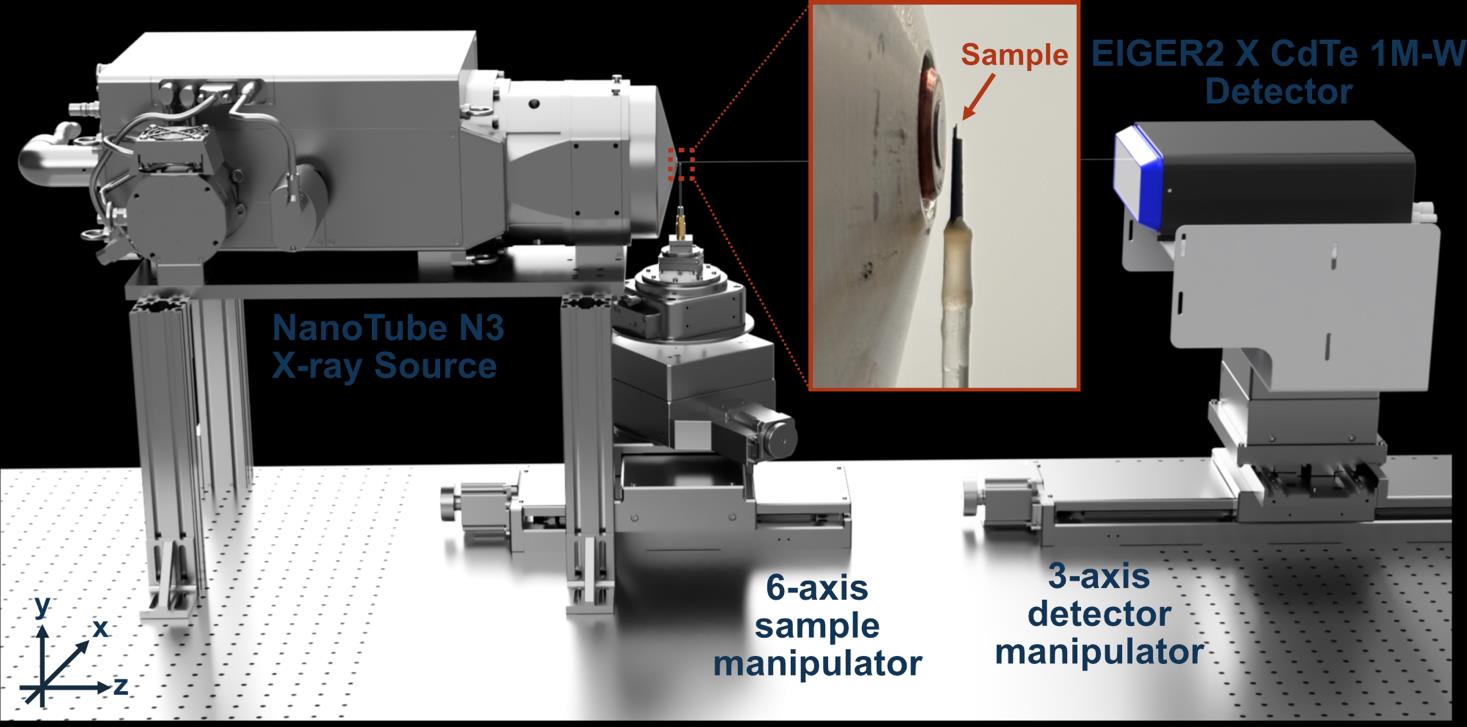
Figure 1: The X-ray nano-CT setup consisting of an Excillum NanoTube N3 X-ray source and a DECTRIS EIGER2 X CdTe 1M-W photon-counting detector, with an inset showing the sample mounted close to the source (Source: Paper, Fig. 1).
For this case study, an AMD Ryzen 7 5800X3D processor was selected as the test sample. This commercial device utilizes hybrid bonding to connect its CPU cores and VCache, featuring internal bonding pads that measure 3 µm in diameter and are arranged with a 9 µm pitch. Because achieving maximum geometric magnification in a nano-CT setup requires a full 360° rotation very close to the X-ray source, the sample size had to be heavily minimized. As illustrated in Figure 2, the initial preparation was performed using a Dremel, followed by precision laser cutting to extract a sub-millimeter pillar containing the exact region of interest.
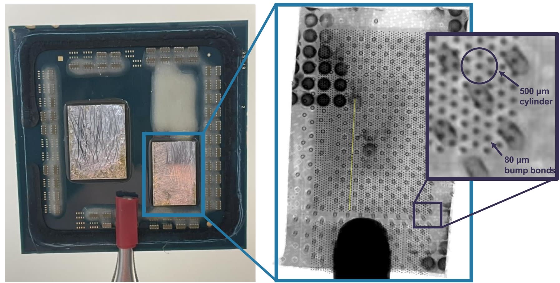
Figure 2: Sample preparation process, highlighting the initial isolation with a Dremel followed by laser cutting to create a sub-millimeter sample suitable for 360° rotation close to the X-ray source (Source: Presentation, Page 8).
The study employed three distinct scanning strategies to evaluate resolution and acquisition efficiency.
- The initial baseline scan utilized a 550 nm X-ray spot at 60 kV with a 5 keV detector energy threshold, capturing 1600 projections over 4.44 hours.
- A second, high-resolution scan optimized the geometric magnification and utilized a smaller 400 nm spot at 80 kV, which successfully reduced the scan time to 2.5 hours.
- Finally, to demonstrate the efficiency of the DECTRIS photon-counting detector, a third scan was performed at an elevated 160 kV with a precise 5-25 keV energy window configured on the detector.
By utilizing this energy window, high-energy photons that do not contribute to image contrast were excluded, allowing the source to run at a higher emission power. This strategy effectively doubled the counted photons passing through the sample—from an average of 2078 to 4126 counts—demonstrating the potential to reduce scan times by 50% while maintaining an identical number of useful photon counts.
The acquired projections were reconstructed using Voxray's Quantum Reconstruction Technique (QRT), an iterative method that solves the Lambert-Beer equation by accounting for the polychromatic X-ray spectrum. The process also applies geometry refinement and total variation denoising to account for sample drift and limited photon flux.
Inspection of Bonding Structures and Layers
The resulting 3D data enables detailed visualization of the component's internal architecture, including redistribution layers, copper pillars, and the hybrid bonding interface. Within the redistribution layers, traces with a width of approximately 200 nm arranged at a 600 nm pitch were clearly resolved.
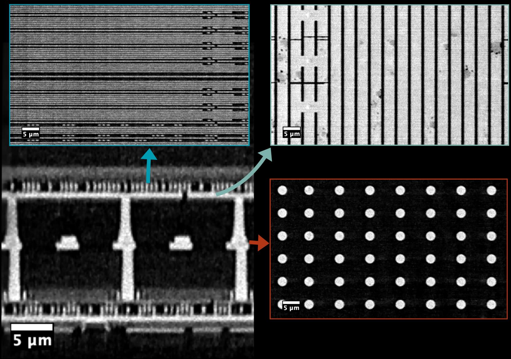
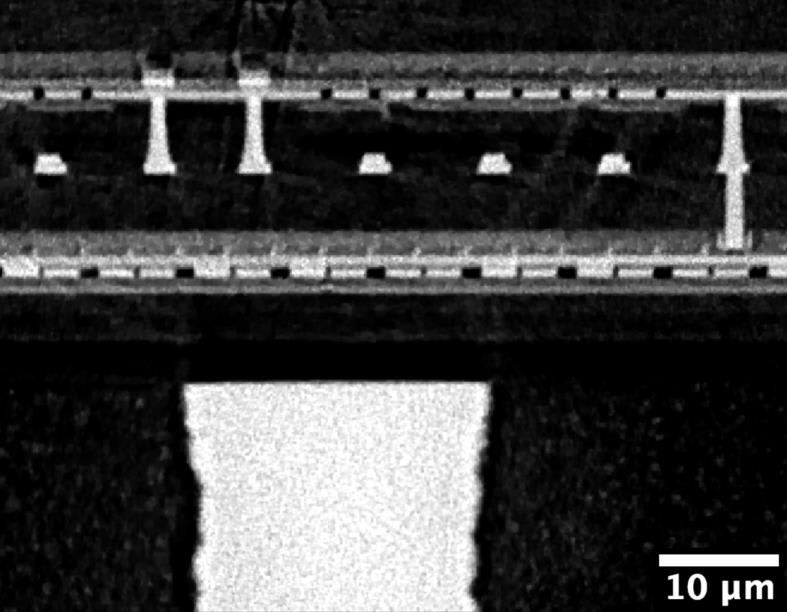
Figure 3: Reconstructed CT slices. Top: horizontal slices through two redistribution layers and the bonding interface, referenced from a vertical cut. Bottom: vertical slice through the hybrid bonding structures.
Inspection of these structures reveals submicron voids and density variations across the bonding pads, as well as localized darker areas indicating potential damage to the metal structure. Vertical slices also demonstrate slight misalignments and shifts in the copper pillars and bonding pads.
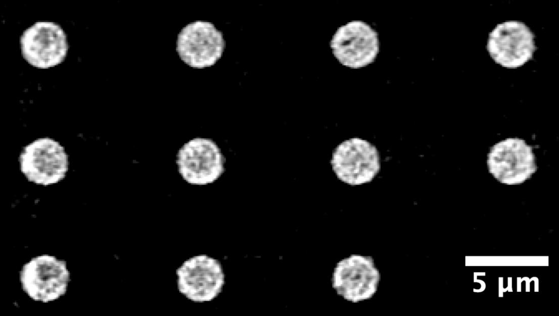
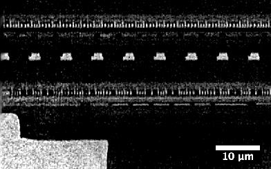
Figure 4: High-resolution QRT slices through the hybrid bonding interface. Top: bonding pads with submicron voids. Bottom: vertical slice showing density variations across the pads.
Metrology and Quantitative Analysis
In addition to visual inspection, QRT provides a clear gray-level separation between the scanned features and the background. This contrast facilitates automated 3D threshold segmentation for metrology. A thickness mesh was calculated to measure the dimensions of the structures by fitting the largest possible spheres into the segmented volumes.
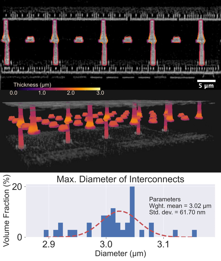
Figure 5: 3D render of segmented hybrid bonds and copper pillars color-coded by component thickness, accompanied by a histogram for quantitative dimensional analysis.
By filtering out objects with an aspect ratio greater than 2 to exclude the copper pillars, 32 individual bonding pads were analyzed. Based on the extracted 3D meshes, the maximum Feret diameter measurements yielded a weighted mean pad diameter of 3.02 µm with a standard deviation of 61.70 nm.
Comparison of Reconstruction Methods: QRT vs. FDK
While the standard Feldkamp-Davis-Kress (FDK) method features shorter processing times—requiring approximately 15 seconds plus 5 to 10 minutes for jitter correction—the iterative QRT method takes approximately 3 hours but offers measurable improvements in image quality.
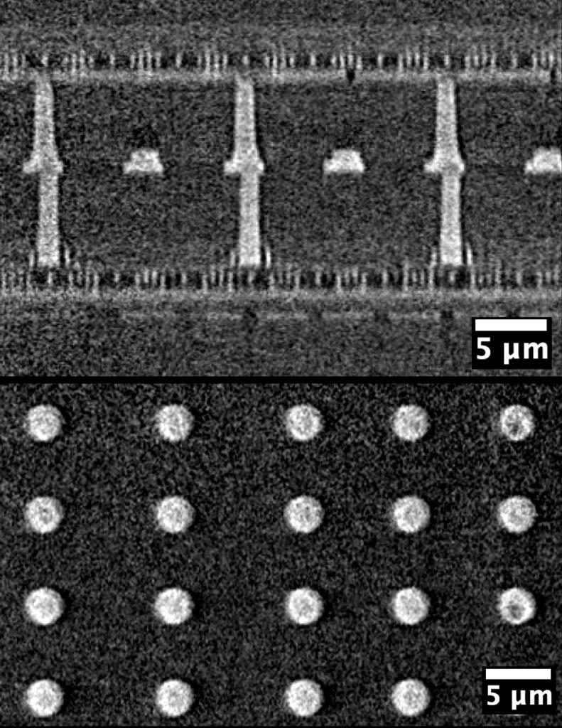
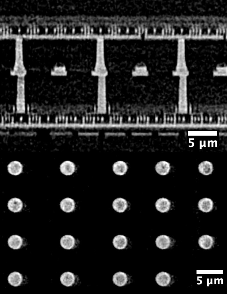
Figure 6: A visual comparison of image quality between a standard FDK reconstruction without denoising (left) and Voxray's iterative QRT reconstruction (right).
In a quantitative comparison of the optimized scan, the QRT reconstruction resulted in a Contrast-to-Noise Ratio (CNR) of 15.81, compared to a CNR of 7.66 achieved via the FDK reconstruction. The difference in gray levels between the features and the background was also higher with QRT, showing a ratio of 13.2 versus 1.7 for FDK. Both reconstructions maintained a similar Signal-to-Noise Ratio (SNR), measured at 12.34 dB for QRT and 12.68 dB for FDK.
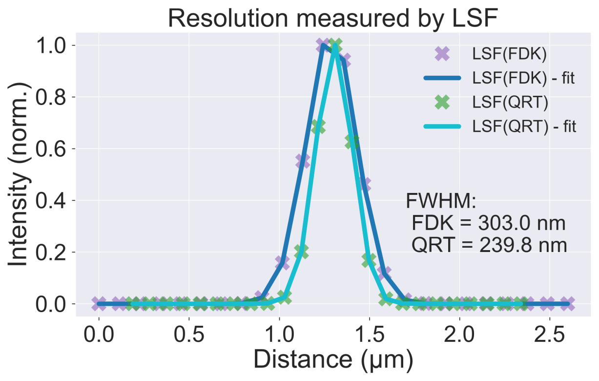
Figure 7: Resolution of the reconstructed volumes measured using the Line Spread Function (LSF) derived from a line profile over a sharp edge.
The physical resolution of the reconstructed slices was measured using the Line Spread Function (LSF). The FDK reconstruction achieved a resolution of 303.0 nm. By incorporating continuous geometry correction during the iteration process, QRT achieved a resolution of 239.8 nm. This metric closely approaches the theoretical resolution limit of 200 nm defined by the 400 nm X-ray source spot size.
As hybrid bonding interconnects continue to scale down, X-ray inspection techniques must advance to meet the demands of advanced semiconductor packaging. This study demonstrates that high-resolution X-ray nano-CT, combining photon-counting detectors with advanced iterative reconstructions like QRT, yields high-quality 3D data capable of identifying submicron voids, structural shifts, and potential delamination. This physical, simulation-based approach ensures reliable datasets for quantitative metrology without the uncertainties of AI-based filtering. While nano-CT is limited by stringent sample size requirements and longer reconstruction times compared to standard FDK, it remains the benchmark for achieving the most accurate 3D volumetric data and the highest possible resolution for failure analysis and process optimization.
This article is based on the research and data presented in the paper "3D Analysis of Hybrid Copper Bonding through X-ray Photon-Counting Nano-CT Imaging," presented at the 2026 IEEE 75th Electronic Components and Technology Conference (ECTC).
https://ieeexplore.ieee.org/document/11561225
Authors:
Till Dreier (Excillum AB)
Darius Rückert (Voxray GmbH)
Spyridon Gkoumas (DECTRIS Ltd.)
Julius Hållstedt (Excillum AB)
The insights and high-resolution data presented in this case study were made possible through extensive collaboration. We gratefully acknowledge Excillum AB for the use of their NanoTube N3 X-ray source and DECTRIS Ltd. for their EIGER2 X CdTe 1M-W photon-counting detector, both of which were instrumental in achieving these imaging results.
Talk to us about QRT or CT-Visualization
Interested in the same reconstruction quality for your semiconductor or nano-CT data? Reach out about QRT, or explore Spectra Web for a secure browser-based CT-viewer.
In this article